Laue & Crystal Orientation
The Laue method helps in determining the orientation of single crystals using white radiation in a reflected or transmitted geometry.
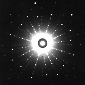
The Laue back reflection mode records X-rays scattered backwards of a sample that has come from a broad-spectrum source. This is useful if the sample is too thick or bulky for X-rays to transmit through it. Each spot can be indexed, i.e. attributed to a specific plane. Crystal orientation is determined from the position of the spots that are generated.
With modern synchrotron and laboratory optics able to deliver micrometre beam size, it is possible to highlight the grain orientation and strain distribution of individual grains in a polycrystalline alloy before and after tensile loading. This solution is also ideal for replacing film-based Laue systems for industrial applications; for example, monitoring for imperfections in high performance turbine blades made from single crystal advanced alloys and this is done to avoid poor creep resistance and failure of blades when at a high operating temperature.
Laue diffraction is a powerful method for investigating crystal orientation.
The Photonic Science & Engineering (PSEL) Laue tool uses a polychromatic “white” beam configuration, passing through the centre of our detector. An intense beam with typically 9-29keV energy range is delivered onto a single crystal material positioned behind the detector. A back reflection geometry is used to record as many Bragg reflections as possible within a single exposure onto a very low noise cooled CMOS based detector.
PSEL Laue tool will deliver a misorientation value against the primary 0-10 reference axis which coincides with the centre of detector and the beam position. It will report specific angular positions for cutting or polishing crystals that will enable specific optical, magnetic or electronic transport properties.
PSEL Laue tool delivers orientation accuracy down to 0.05 degrees, this is critical for semiconductor detectors, sapphire substrates, laser or gamma scintillation materials, ceramics and metal alloys.
Thanks to a beam footprint as small as <0.5mm on the sample, crystals with dimensions as small as a few millimetres can be checked in the laboratory.
The Photonic Laue Systems is widely in the Semiconductor industry for Wafer fabrication: GaN Wafers, SiC Wafers,GaAs Wafers, Compound Semiconductors, Germanium Wafers, CdZnTe Wafers, and Silicon Wafers.
We Recommend...
X-ray Laue Back-Scattered Camera Laue Crystal Orientation System

Contact Us
22 Theaklen Drive,
Saint Leonards-on-sea,
TN38 9AZ,
United Kingdom


