News
Laue Crystal Orientation System used in ESRF Micro-Diffraction Experiment
7th Jul, 2020
Laue diffraction is a powerful method for investigating crystal orientation. We’ll discuss in this short case study acquisition routines deployed in research as well as production laboratories.
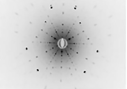
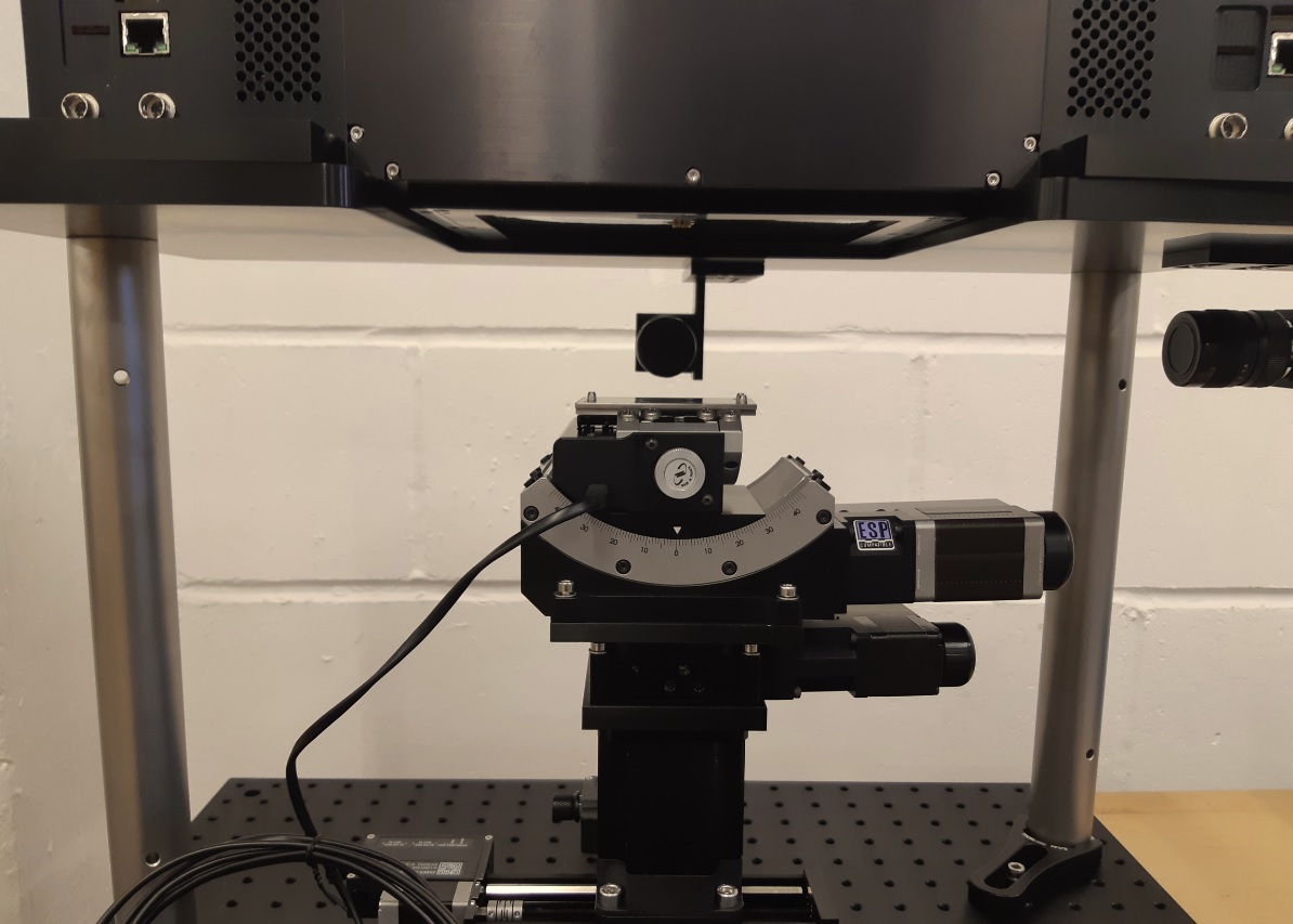
Figure 1. Sapphire C-axis aligned with 0.05 degree accuracy
The Photonic Science & Engineering (PSEL) Laue tool uses a polychromatic “white” beam configuration, passing through the centre of our detector. An intense beam with typically 9-29keV energy range is delivered onto a single crystal material positioned behind the detector. A back reflection geometry is used to record as many Bragg reflections as possible within a single exposure onto a very low noise cooled CMOS based detector.
PSEL Laue Crystal Orientation tool will deliver a misorientation value against the primary 0-10 reference axis which coincides with the centre of detector and the beam position. It will report specific angular positions for cutting or polishing crystals that will enable specific optical, magnetic or electronic transport properties.

Figure 2. Sapphire on motorized goniometer
PSEL Laue tool delivers orientation accuracy down to 0.05 degree, this is critical for semiconductor detectors, sapphire substrates (Figure 1), laser or gamma scintillation materials, ceramics and metal alloys.
Thanks to a beam footprint as small as <0.5mm on the sample, crystals with dimensions as small as a few millimetres can be checked in the laboratory.
Wafer samples, diamond or silicon seed samples orientation are checked using a vertical beam geometry and motorized goniometer (Figure 2). Samples grown out from the seeds are then tested against the desired orientation using motorized scanning stages.
Over 100 samples are tested per batch, misorientation values, distance to the closest nodal spots amongst the three main directions: ie 100 110 and 111 (Figure 4) are delivered in a single file ready to be processed for further analysis and QA controls.
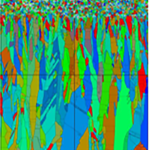
Figure 3.Polysilicon brick
Figure 5 Mono like wafer
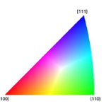
Figure 4 Euler triangle
Smaller beam delivery are used for checking sub grain structures, with beam size down to <200 µm. The PSEL Laue tool can then be used for mapping specific multi grain structures and grain boundaries to produce an orientation map.
Unlike EBSD, these maps can be generated from large scale samples using automatic scanning routines with up to 20,000 measurement points per batch. This is particularly useful in the case of polycrystalline samples, multi phased alloys, where grain analysis, seed growth mechanism can be refined and modelled.
An example of automatic scanning routine is displayed in (Figure 5) for mono-like solar grade Silicon wafers and for polycrystalline bulk Silicon (Figure 3). Grains contours, centre of gravity coordinates are extracted automatically for each grain.
The PSEL Laue tool uses 2 dimensional heavy duty high resolution motorized gantry to position each grain accurately under the X-ray beam, with typical duty cycle of 6 seconds per measurement point. Faster routines with smaller beam size are available at the synchrotron.
A case study using PSEL latest X-ray sCMOS detectors is highlighted below, courtesy from one of the most advanced LAUE microdiffraction beamline in operation at the European Synchrotron Research Facility:
ESRF CRG/BM32/Microdiffraction

We present ongoing development and studies of in situ Differential Aperture X-ray Microscopy (DAXM) performed on micropillars during mechanical test. Few number of deformation fatigue cycles are performed and simultaneously Laue patterns are recorded each step to capture the evolving microstructure by 2D map and 3D volume.
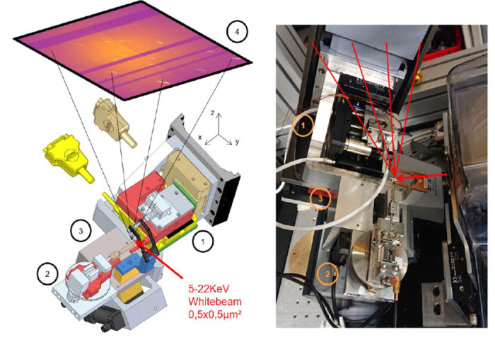
Figure 6 Setup of the in situ Straning Device 3D X-ray Laue microscope on BM32. Microsized sample are held by left part (2) and deformed by actuators from the right one (3). A fork with one several wires can be moved independently by stages (3).
To understand the fundamental structural damage mechanisms of materials under fatigue load at the mesoscale, direct observations of atomic lattices transform are required. When decreasing objects size, dislocations interactions with grain boundaries and sample surface govern dominate the mechanical behavior. Accurate predictive laws and experimental data are needed to model and optimize this new class of grain boundaries engineering materials. Two major needs are required in this field: (1) access to structural parameters inside materials not only at its surface (e.g. by electronic microscopy), (2) the ability to follow the evolution of the same microstructure to get rid of experimental artefacts and for a better reliability in the interpretation of structural quantitative changes. Therefore in situ mechanical test save time (no sample realignment) and bring a better control of experiment geometry. The XMicroFatigue measurements campaigns were focused on the first fatigue cycles to observe a few number of dislocations and how they accumulate at a single grain boundary (or transmit through it). Two premiers have been done and will be published soon: (1) 3D map (1 µm3 voxel) on a microsized object and (2) in situ monitoring of 3D microstructure evolution (6 hours/3D map of 10*10*15 µm3 with lateral resolution of 0.5×0.5 µm and depth resolution less than 1 µm).
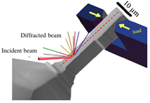
Figure 7 (left) X-ray scattering (detector on top),
Photonic Science large area X-ray sCMOS camera 150 x 150 mm 4K x 4K
The following experimental protocol was used during in situ experiments (Figure 8) : The samples were submitted to one full fatigue cycle. During in situ loading mechanical data (force and displacement) and μLaue patterns were recorded simultaneously. The three dimensional scans were performed in the undeformed state (0 cycles) and, then, after 1⁄4, 1⁄2, 3⁄4 and 1 cycle in order to thoroughly investigate the local fatigue structure formed in single and bi-crystalline microsamples. During 3D scans a volume of ~10x10x15μm3 was scanned with the DAXM setup with a step size of 1μm and a polychromatic beam (5 to 22 keV), 0,5×0,5μm2 sized. In Fig.8, a schematic reconstruction of a 3D volume scan is shown. The analysis was performed on one out of eight bi-crystalline sample. The analysis of acquired data is still ongoing, but already now it is clear that the data contains unique information on the 3D evolving microstructure of our material. We are confident to quantitatively assess local density of GND’s, the local deviatoric strain and misorientations at the grain boundary (Figure 8). Data treatment and analysis are still ongoing.
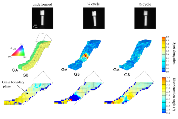
Figure 8: Microstructural evolution of (5X5x25 µm3) micropillar composed by 2 grains GA and GB (whose misorientation corresponds to an impenetrable high-angle grain boundary) during the first steps of fatigue cycle. Each column correspond to a given deformation step (central column with the highest strain). First row: visible light images of the pillar. Second row: (left) 3D orientation map. (middle and right) 3D map of Laue spot elongation related to dislocations storage volumic density. (right) Initial microstructure is almost recovered in terms of defects (damages) density. Third row: 2D GA/GB misorientation map at the grain boundary plane de cross section. (right) The remaining fine internal misorientation heterogeneities (introduced by crystalline defects) can be used in dislocations dynamical simulations to calibrate and improve greatly interactions potentials.
Further information on Laue detectors
You may also be interested in X-ray Detectors for Synchrotron Beamlines
References
J. Eymery, O. Ulrich, J.-S. Micha, O. Robach
Univ. Grenoble Alpes, CEA-INAC, F-38000 Grenoble, France
Christoph Kirchlechner
KIT, 76131 Karlsruhe, Germany
Daniel Brau
Photonic Science & Engineering, TN38 9AZ, St Leonards, UK
![]()