News
SWIR cameras- Dark Luminescence, a new modality for sorting high efficiency solar wafer and solar cells
19th May, 2020
Production of High efficiency solar panels depend on strict selection of the highest quality grade bare silicon wafers as well as processed cells with the lowest defect density.
Current sorting inspection tools are based on CCD or CMOS cameras and are only capable of capturing the tail of electroluminescence or photoluminescence peak signals emitted beyond 900nm, due to limited sensitivity beyond 1,100nm.
Photonic science Short Wave Infra Red (SWIR) tools, thanks to high quantum efficiency, will integrate the full intensity from the primary silicon band gap emission, allowing better contrast defect classification under low reverse bias current conditions when electroluminescence is used, or lower excitation wattage when photoluminescence is used.
Our SWIR tools will also capture secondary band gap emissions under forward bias current conditions, well beyond the silicon band gap, unveiling dislocation / impurities as well as sub band recombination defects that will normally remain invisible to traditional CCD or CMOS camera based systems and compromise solar cell efficiency.
Delivering enhanced classification capabilities for the highest solar grade wafers / processed cells will potentially depend on simultaneous capture of both primary and secondary band gap emission measurements within a single tool now available from Photonic Science.
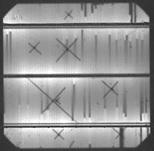
Monocrystalline cell, EL 512×512 image resolution acquired in 100ms, 2A with cooled InGaAs camera. Low current stress / high contrast from minority carriers
9 ms exposure, primary band gap emission on finished cell with 6.5A current
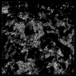
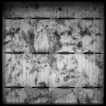
80 ms exposure, secondary band gap emission on finished cell, unveiling “invisible” grain boundaries and dislocations
If you are interested in leveraging the benefits of SWIR imaging for your application, simply contact a member of the Photonics Science team today for SWIR camera quotes.