News
2D Orientation Mapping of Silicon Wafers with Laue Diffraction
4th Jul, 2022
2D Orientation Mapping of Silicon Wafers with Laue Diffraction
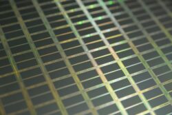
Silicon wafers form the basis of modern microelectronics and photovoltaic technology. They need highly accurate alignment with regards to their crystalline orientation when they undergo various processing steps. It is possible to determine the crystalline structure of a silicon wafer with a hammer and nail—but this is obviously not the recommended approach. Instead, you need an accurate non-destructive tool that is precise, fast (real-time capability), and requires no sample preparation in advance. That solution is Laue diffraction.
Silicon Wafer: Orientation defines Properties
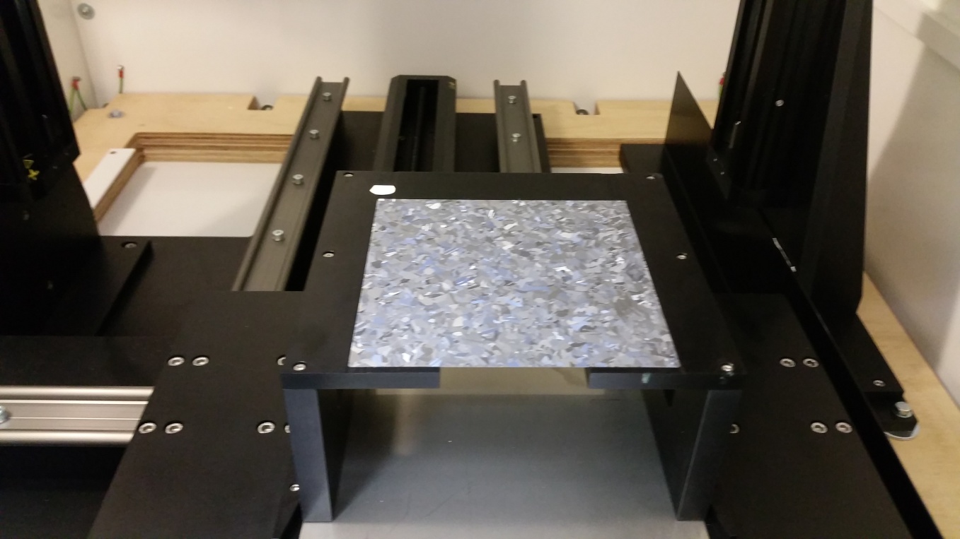
Before we give you a brief introduction to orientation mapping of silicon wafers with Laue diffraction, let us talk about some more about wafer material basics. Wafers are thin slices of semiconducting material grown in a regular crystal structure. When sliced, the surface is aligned in one of several different orientations. The orientation of a standard silicon wafer is qualified using Miller indices and marked by a notch on the wafer’s edge which allows for the identification of its direction of orientation. Silicon wafers for microelectronics are generally monocrystalline. Though, in silicon photovoltaics some solar cells are made of polycrystalline wafers which consist of micrometre sized crystalline grains.
Orientation mapping with Laue Diffraction
The general principle of the Laue diffraction technique is based on a polychromatic X-ray beam that impinges on the crystal. The reflected X-ray beam is recorded on a Laue detector, for example on an X-ray sensitive sCMOS camera. Due to diffraction of the X-ray beam on the crystal sample, a particular Laue spot pattern is formed on the detector plane. The complex pattern is usually analyzed by software tools.
To achieve 2D mapping with Laue diffraction, the X-ray beam needs to be tightly focused on the sample. The smaller the focal spot size, the higher the spatial resolution of the Laue diffraction measurement. By scanning the X-ray focus over the plane sample, a 2D crystal orientation map can be created. One amongst many potential applications is the 2D orientation mapping of a polycrystalline silicon solar cell wafer for photovoltaics. The structure and orientation of individual silicon grains is strongly linked to the efficiency of the solar cell. Therefore, Laue diffraction provides an ideal method of mapping the orientation of grains in polycrystalline solar cell wafers.
Photonics Science provides a crystal orientation Laue diffraction system for industrial and scientific applications. The back reflection system based on Laue diffraction achieves real-time crystal orientation measurement accuracy down to 0.1 degrees and mis-orientation measurement accuracy down to 0.05 degrees. The beam size of the X-ray beam is no greater than 200 µm to achieve extremely small spot sizes on the sample. Applying the Photonic Science Laue system on a large polycrystalline wafer sample, up to 10,000 orientation measurements can be recorded automatically.
You can gain further insights into Laue cameras of the system from our MD Daniel Brau. Or, if you have any questions, why not contact a member of the team today?