News
Silicon Wafers – Grain Orientation Mapping
8th Jun, 2020
Understanding the propagation of dislocations, and formation of sub grain structure / boundaries during the production of mono like bulk Silicon is fundamental for delivering low cost high efficiency solar cells.
Mapping grain orientation and grain structure are traditionally done using Electron Back Scattered Diffraction but is limited to small areas. The Photonic Science X-ray Laue system is capable of mapping / imaging grain structure as well as grain orientation over 156 x 156mm active area with typically 220 microns resolution.
If you would like more information about our comprehensive range of Laue X-ray imaging products, simply contact a member of the team today.

Mono-like silicon wafer
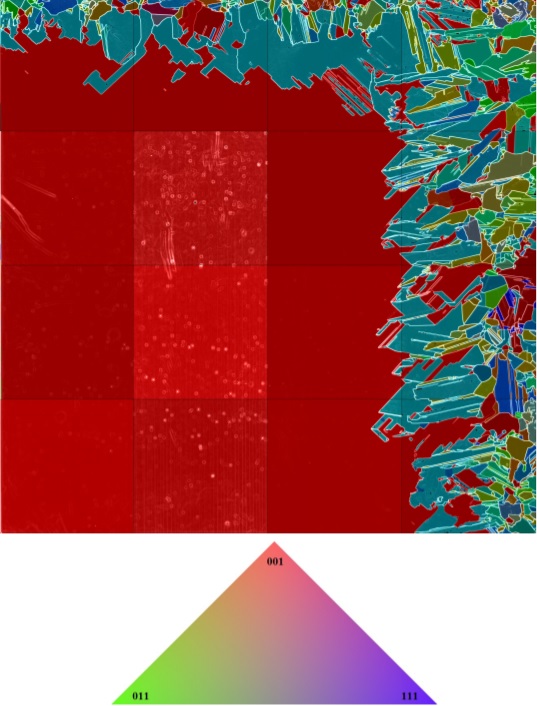
Mono-like silicon wafer

